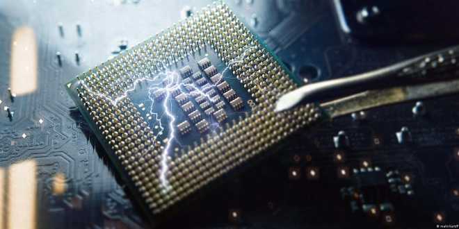
For the first time, scientists have succeeded in creating a functional and scalable graphene-based semiconductor.
This breakthrough paves the way for a potential transformation in the computing world, potentially leading to computers that are faster and more efficient than the existing silicon chip technology.
Semiconductor chips are becoming increasingly central to the global economy, often likened to the ‘new oil’ of the tech era. These chips, integral from data centers to smartphones, are essential across all economic sectors.
The team, led by Walter de Heer, Regents’ Professor of Physics at Georgia Tech, in collaboration with researchers from Atlanta, Georgia, and Tianjin, China, developed a graphene semiconductor compatible with standard microelectronics processes. This compatibility is vital for any technology aiming to replace silicon, according to a statement from the Georgia Institute of Technology.
Graphene, a material comprising a single layer of carbon atoms, is known for its exceptional strength, surpassing steel at similar thicknesses. It also conducts electricity well and is highly resistant to heat and acids.
Despite these benefits, the development of an effective graphene semiconductor has been challenging. A key hurdle has been graphene’s lack of a bandgap, essential in semiconductors for controlling electron flow.
Previous research showed graphene’s potential as a semiconductor on a small scale, but scaling up to the size needed for practical computer chips was problematic.
Walter de Heer’s team at Georgia Tech made a breakthrough by using silicon carbide wafers. They heated these wafers to evaporate the silicon, leaving behind graphene with a bandgap. They even created a working transistor, a crucial component that acts as an on/off switch for current flow.
Their process, similar to the methods used for silicon chips, suggests potential for scaling up the technology. David Carey from the University of Surrey, UK, noted the significance of using wafers, as it aligns with the semiconductor industry’s standard practices, making the process scalable.
This advancement is particularly important as silicon, the backbone of most modern electronics, is nearing its limits due to demands for faster computing and smaller devices.